
Madhya Pradesh Semiconductor Summit Focuses on Advanced Chip Packaging, Testing Ecosystem
Madhya Pradesh Semiconductor Summit, 2026 in Indore focused on the development of advanced packaging and testing, a strong fabless ecosystem, and semiconductor manufacturing and supply chains.

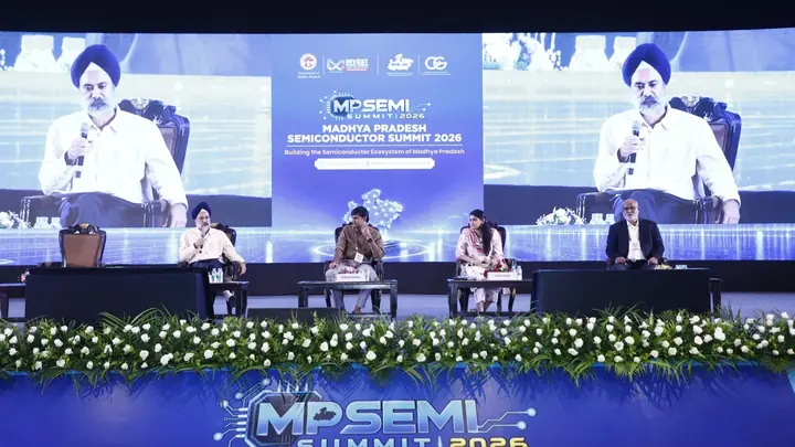
Madhya Pradesh Semiconductor Summit, 2026 in Indore focused on the development of advanced packaging and testing, a strong fabless ecosystem, and semiconductor manufacturing and supply chains. Industrialists and experts from the semiconductor sector took part in three panel discussions at the summit.
Indore, 23 October 2026.
The discussions examined the possibilities of developing Madhya Pradesh as a centre for advanced packaging and testing, building a strong fabless ecosystem in the state, and strengthening semiconductor manufacturing and supply chains.
Experts discussed the arrangements needed to develop the complete value chain, from chip design and product development to fabrication, packaging and testing. Industrial infrastructure, supportive policies, financial resources, market availability, cooperation between industry and educational institutions, advanced research and skill development were identified as key requirements.
The first panel discussion was held on the subject of making Madhya Pradesh a centre for advanced packaging and testing. The discussion was moderated by Tata Electronics Senior Vice-President Charan Gurumurthy.
The experts discussed the facilities available for setting up industries in the state, technical institutions, policy support and the requirements of the packaging industry. The discussion also focused on the infrastructure and local capabilities that would be needed to establish and expand semiconductor packaging operations.
Santosh Kumar, Chief Executive Officer of Paras Semiconductor, said Madhya Pradesh was an ideal location for setting up the semiconductor industry. He said the Indore, Ujjain corridor was being developed as a semiconductor zone.
According to Kumar, land, water and electricity were available for setting up plants in the corridor, along with cargo and logistics facilities. He said the ecosystem and supply chain required for the industry were also developing in the state.
Kumar said the support of the Madhya Pradesh government, its quick decision-making process and the availability of speedy approvals through the single-window system were creating a favourable environment for setting up industries.
Speaking about the development of infrastructure for the packaging industry, Kumar said the expertise of global companies that provide comprehensive engineering services from the beginning to the end of plant design and construction could be used. He said design and construction requirements could be met through coordination between these companies and local contractors.
Apurva Raut, Chief Technology Officer of RRP Electronics, said the development of the semiconductor packaging industry required the right approach and continuity in efforts. She said both these features were present in Madhya Pradesh.
Raut described the availability of electricity as a critical requirement for the industry. She said Madhya Pradesh being a power-surplus state made it an important location for the semiconductor industry.
She said the state needed to develop the capacity to handle cargo and logistics operations on a large scale according to the requirements of the packaging industry. Better connectivity with major cities would also have to be ensured, she said.
Raut suggested that memorandums of understanding, or MoUs, should be signed with IITs and other universities in the field of packaging design. Such cooperation was discussed in the context of developing the skills and technical capabilities needed by the packaging industry.
Sudhir Naik referred to the technical talent available in the state. He said progressive institutions such as IIT Indore and engineering colleges provided the foundation for developing Madhya Pradesh as a centre of technical talent.
Naik stressed the need to promote research and development in advanced packaging. He said the related technology and services should be available locally at a reasonable cost.
He also said that a strong and reliable supply chain would be necessary to meet the requirements of the industry. The availability of local technical capabilities and dependable suppliers was discussed as part of the wider infrastructure needed for packaging and testing.
Vineet K. Singh, Chief Executive Officer and Managing Director of H-Semi Products, Singapore, said a semiconductor packaging ecosystem was developing in Madhya Pradesh. He said OSAT companies were also coming to the state.
Singh said the state government was implementing policies at a fast pace, and that this was giving momentum to the development of the sector. The discussion linked the growth of the packaging ecosystem with policy execution, infrastructure and the arrival of companies working in the sector.
The second panel discussion focused on building a strong fabless ecosystem in Madhya Pradesh. The discussion was moderated by Satya Gupta, President of the VLSI Society of India.
The panel examined the support required from chip design to product development, the challenges faced by fabless companies, customer requirements, marketing and policy arrangements.
Jatinder Singh said a strong fabless ecosystem required better and high-quality products to be developed through chip design. He said improved product quality would also increase the possibilities of higher revenue for fabless companies.
Singh said companies should give special attention to the satisfaction of the final consumer. He also described the availability of skilled and experienced talent at the senior level as necessary for the development of the sector.
He stressed the need to strengthen the product development ecosystem in Madhya Pradesh. He also called for the support required for product development to be included in the policy framework.
Jaswinder Ahuja, Adviser to the India Semiconductor Mission, said the availability of financial resources was a major challenge for fabless companies. He said companies needed to move beyond chip development and grow as companies that developed complete products.
Ahuja said a comprehensive ecosystem supporting product development should be created. This would allow companies to take their designs to the market in the form of useful products.
The discussion also covered the need for support at different stages of product development. The focus was on ensuring that a chip design could be taken forward through development and then made available as a product for customers.
Preet Yadav said the service sector had received special attention for several years. He said it was now necessary to focus on the manufacturing sector as well.
Yadav said fabless companies should pay special attention to the backend processes of product design. This, he said, would help meet the requirements related to product development and manufacturing more effectively.
The emphasis on backend processes connected chip design with the practical requirements of developing and manufacturing products. The discussion highlighted the need for fabless companies to build capabilities beyond design so that their products could move towards manufacturing and the market.
Jyotis Indirabhai, Chief Executive Officer and Co-founder of Netrasemi Private Limited, said the product development ecosystem would have to mature for the fabless ecosystem to become stronger.
He said it was necessary to ensure the quality of production and the availability of markets for products. In his view, the strength of the fabless ecosystem depended not only on technical capability but also on the ability to produce quality products and find markets for them.
Manoj Agrawal said technical capability was available for fabless companies. He added that an appropriate system should also be developed for marketing their products.
The second panel therefore placed equal emphasis on product quality, financial resources, experienced talent, product development, marketing and market access. The experts discussed these areas in relation to the ability of fabless companies to grow and take their designs to customers.
The third panel discussion was held on semiconductor manufacturing and supply chains. Experts discussed expanding the country’s manufacturing capabilities, research into advanced technologies, centralised experimental facilities and skill development according to the requirements of industry.
Dr Kamaljit Singh, Director General of Semiconductor Lab, Mohali, described manufacturing and a strong supply chain as extremely important and sensitive components of the semiconductor industry.
He said strengthening the complete value chain, from chip designing to fabrication and packaging, was essential for the success of the industry. The discussion treated manufacturing and supply chains as connected parts of the same semiconductor ecosystem.
Mukesh Kumar, Professor at IIT Indore, stressed the need to expand India’s capabilities in semiconductor manufacturing. He said India was currently established as a strong centre for chip design.
Kumar said that, keeping future requirements in mind, the country now needed to move beyond 2D semiconductors and focus on advanced technologies such as quantum computing.
He also highlighted the need to promote experimental facilities, experimental research and skill enhancement in educational institutions. According to Kumar, these capabilities would be important for expanding India’s role in semiconductor manufacturing and for preparing institutions to address future requirements.
Kumar said product quality and reliability were extremely important in the semiconductor sector. For this, he called for the creation of a strong state-sponsored research and development system in the country.
Alpa Sood, Country Manager of Teradyne, stressed the need to prepare students according to the future requirements of the semiconductor and electronics manufacturing sectors.
She said advanced training for students was extremely necessary to meet the growing requirements of the sector. Her comments focused on aligning education and training with the technical capabilities needed in semiconductor and electronics manufacturing.
The ideas presented during the panel discussions pointed to the need for a strong ecosystem connecting chip design, product development, manufacturing, packaging and testing for the overall development of the semiconductor industry in Madhya Pradesh.
For advanced packaging and testing, the availability of land, water, reliable power supply, better transport connectivity, cargo and logistics facilities, clean rooms and local technical services was identified as important.
The experts also highlighted the requirements of fabless companies. These included financial resources, experienced talent, quality products, improvement based on customer feedback, and support for markets and marketing.
The discussions brought together infrastructure, policy, research, skills, product development and supply chain requirements across the semiconductor sector. The focus remained on building capabilities within Madhya Pradesh while connecting the state’s technical institutions, industries, local contractors, markets and supply chain facilities with the wider semiconductor value chain.
Frequently asked questions
What was the focus of the Madhya Pradesh Semiconductor Summit 2026?
The summit focused on advanced chip packaging and testing, a strong fabless ecosystem, and semiconductor manufacturing and supply chains.
Where was the Madhya Pradesh Semiconductor Summit 2026 held?
The summit was held in Indore on 23 October 2026.
What requirements were identified for developing Madhya Pradesh’s semiconductor ecosystem?
Key requirements included industrial infrastructure, supportive policies, financial resources, market availability, industry-education cooperation, advanced research, and skill development.
What was the subject of the first panel discussion?
The first panel discussed making Madhya Pradesh a centre for advanced packaging and testing.
Which corridor was being developed as a semiconductor zone?
According to Paras Semiconductor CEO Santosh Kumar, the Indore-Ujjain corridor was being developed as a semiconductor zone.
You may also like
 Madhya Pradesh
Indore Administration Uses Bulldozers, Clears 50,000 Sq Ft Near Airport
 Madhya Pradesh
Indore Civic Body Imposes ₹2,000 Fine for Wasting Water in City
 Madhya Pradesh
Successful Engine Trial Advances Indore-Dahod Rail Link, Safety Inspection Next
 Madhya Pradesh
Indore Mayor Launches Water-Waste Monitoring Drive, Warns Of Challans For Repeat Offenders
Most read
- 1
Xi Orders Urgent Rescue Efforts After Tibet Earthquake Kills 16, Injures 54
- 2
Schools Shut in Five Tamil Nadu Districts, Including Chennai, Amid Heavy Rain
- 3
Hong Kong Insurance Authority Tightens Premium Financing Oversight as Risks Emerge
- 4
Madanpur Masters Beat Firozabad Fighters by Two Runs in T-10 Opener
- 5
eMudhra Certificate: 8 weak certificates raise Internet Security concerns as browsers act
Comments
No comments yet. Be the first to comment.